- 您现在的位置:买卖IC网 > Sheet目录2004 > LTC1746IFW#TRPBF (Linear Technology)IC ADC 14BIT 25MSPS LP 48TSSOP
14
LTC1746
1746f
APPLICATIO S I FOR ATIO
WU
UU
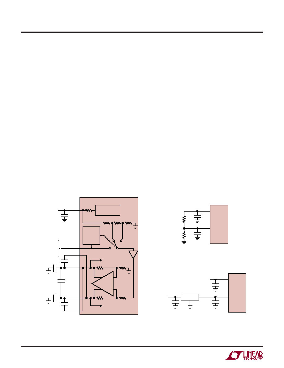
Reference Operation
Figure 5 shows the LTC1746 reference circuitry consisting
of a 2.35V bandgap reference, a difference amplifier and
switching and control circuit. The internal voltage refer-
ence can be configured for two pin selectable input ranges
of 2V(
±1V differential) or 3.2V(±1.6V differential). Tying
the SENSE pin to ground selects the 2V range; tying the
SENSE pin to VDD selects the 3.2V range.
The 2.35V bandgap reference serves two functions: its
output provides a DC bias point for setting the common
mode voltage of any external input circuitry; additionally,
the reference is used with a difference amplifier to gener-
ate the differential reference levels needed by the internal
ADC circuitry.
An external bypass capacitor of 4.7
F or larger is required
for the 2.35V reference output, VCM. This provides a high
frequency low impedance path to ground for internal and
external circuitry. This is also the compensation capacitor
for the reference. It will not be stable without this
capacitor.
The difference amplifier generates the high and low refer-
ence for the ADC. High speed switching circuits are
connected to these outputs and they must be externally
bypassed. Each output has two pins: REFHA and REFHB
for the high reference and REFLA and REFLB for the low
reference. The doubled output pins are needed to reduce
package inductance. Bypass capacitors must be con-
nected as shown in Figure 5.
Other voltage ranges in between the pin selectable ranges
can be programmed with two external resistors as shown
in Figure 6a. An external reference can be used by applying
its output directly or through a resistor divider to SENSE.
It is not recommended to drive the SENSE pin with a logic
device since the logic threshold is close to ground and
VDD. The SENSE pin should be tied high or low as close to
the converter as possible. If the SENSE pin is driven
externally, it should be bypassed to ground as close to the
device as possible with a 1
F ceramic capacitor.
VCM
REFHA
REFLB
SENSE
TIE TO VDD FOR 3.2V RANGE;
TIE TO GND FOR 2V RANGE;
RANGE = 2 VSENSE FOR
1V < VSENSE < 1.6V
2.35V
REFLA
REFHB
4.7
F
4.7
F
INTERNAL ADC
HIGH REFERENCE
BUFFER
0.1
F
1746 F05
LTC1746
4
DIFF AMP
1
F
1
F
0.1
F
INTERNAL ADC
LOW REFERENCE
2.35V BANDGAP
REFERENCE
1.6V
1V
RANGE
DETECT
AND
CONTROL
Figure 5. Equivalent Reference Circuit
VCM
SENSE
2.35V
1.1V
4.7
F
12.5k
1
F
11k
1746 F06a
LTC1746
VCM
SENSE
2.35V
5V
1.25V
6
4
1, 2
4.7
F
1
F
0.1
F
1746 F06b
LTC1746
LT1790-1.25
Figure 6a. 2.2V Range ADC
Figure 6b. 2.5V Range ADC with an External Reference
发布紧急采购,3分钟左右您将得到回复。
相关PDF资料
LTC1747IFW#PBF
IC ADC 12BIT 80MSPS 48-TSSOP
LTC1748CFW#TRPBF
IC ADC 14BIT 80MSPS 48-TSSOP
LTC1749IFW#PBF
IC ADC 12BIT 80MSPS SMPL 48TSSOP
LTC1750IFW#PBF
IC ADC 14BIT 80MSPS SMPL 48TSSOP
LTC1799HS5#TRPBF
IC OSC SILICON 33MHZ TSOT23-5
LTC1821ACGW
IC D/A CONV 16BIT PRECISE 36SSOP
LTC1851CFW
IC ADC 12BIT 1.25MSPS 48-TSSOP
LTC1853IFW#TRPBF
IC A/D CONV 8CH 12BIT 48-TSSOP
相关代理商/技术参数
LTC1747CFW
功能描述:IC ADC 12BIT 80MSPS 48-TSSOP RoHS:否 类别:集成电路 (IC) >> 数据采集 - 模数转换器 系列:- 标准包装:1 系列:- 位数:14 采样率(每秒):83k 数据接口:串行,并联 转换器数目:1 功率耗散(最大):95mW 电压电源:双 ± 工作温度:0°C ~ 70°C 安装类型:通孔 封装/外壳:28-DIP(0.600",15.24mm) 供应商设备封装:28-PDIP 包装:管件 输入数目和类型:1 个单端,双极
LTC1747CFW#PBF
功能描述:IC ADC 12BIT 80MSPS 48-TSSOP RoHS:是 类别:集成电路 (IC) >> 数据采集 - 模数转换器 系列:- 产品培训模块:Lead (SnPb) Finish for COTS
Obsolescence Mitigation Program 标准包装:2,500 系列:- 位数:12 采样率(每秒):3M 数据接口:- 转换器数目:- 功率耗散(最大):- 电压电源:- 工作温度:- 安装类型:表面贴装 封装/外壳:SOT-23-6 供应商设备封装:SOT-23-6 包装:带卷 (TR) 输入数目和类型:-
LTC1747CFW#TR
功能描述:IC ADC SMPL 12BIT 80MSPS 48TSSOP RoHS:否 类别:集成电路 (IC) >> 数据采集 - 模数转换器 系列:- 标准包装:1 系列:- 位数:14 采样率(每秒):83k 数据接口:串行,并联 转换器数目:1 功率耗散(最大):95mW 电压电源:双 ± 工作温度:0°C ~ 70°C 安装类型:通孔 封装/外壳:28-DIP(0.600",15.24mm) 供应商设备封装:28-PDIP 包装:管件 输入数目和类型:1 个单端,双极
LTC1747CFW#TRPBF
功能描述:IC ADC 12BIT 80MSPS 48-TSSOP RoHS:是 类别:集成电路 (IC) >> 数据采集 - 模数转换器 系列:- 产品培训模块:Lead (SnPb) Finish for COTS
Obsolescence Mitigation Program 标准包装:2,500 系列:- 位数:12 采样率(每秒):3M 数据接口:- 转换器数目:- 功率耗散(最大):- 电压电源:- 工作温度:- 安装类型:表面贴装 封装/外壳:SOT-23-6 供应商设备封装:SOT-23-6 包装:带卷 (TR) 输入数目和类型:-
LTC1747IFW
功能描述:IC ADC SMPL 12BIT 80MSPS 48TSSOP RoHS:否 类别:集成电路 (IC) >> 数据采集 - 模数转换器 系列:- 标准包装:1 系列:- 位数:14 采样率(每秒):83k 数据接口:串行,并联 转换器数目:1 功率耗散(最大):95mW 电压电源:双 ± 工作温度:0°C ~ 70°C 安装类型:通孔 封装/外壳:28-DIP(0.600",15.24mm) 供应商设备封装:28-PDIP 包装:管件 输入数目和类型:1 个单端,双极
LTC1747IFW#PBF
功能描述:IC ADC 12BIT 80MSPS 48-TSSOP RoHS:是 类别:集成电路 (IC) >> 数据采集 - 模数转换器 系列:- 产品培训模块:Lead (SnPb) Finish for COTS
Obsolescence Mitigation Program 标准包装:2,500 系列:- 位数:12 采样率(每秒):3M 数据接口:- 转换器数目:- 功率耗散(最大):- 电压电源:- 工作温度:- 安装类型:表面贴装 封装/外壳:SOT-23-6 供应商设备封装:SOT-23-6 包装:带卷 (TR) 输入数目和类型:-
LTC1747IFW#TR
功能描述:IC ADC SMPL 12BIT 80MSPS 48TSSOP RoHS:否 类别:集成电路 (IC) >> 数据采集 - 模数转换器 系列:- 标准包装:1 系列:- 位数:14 采样率(每秒):83k 数据接口:串行,并联 转换器数目:1 功率耗散(最大):95mW 电压电源:双 ± 工作温度:0°C ~ 70°C 安装类型:通孔 封装/外壳:28-DIP(0.600",15.24mm) 供应商设备封装:28-PDIP 包装:管件 输入数目和类型:1 个单端,双极
LTC1747IFW#TRPBF
功能描述:IC ADC 12BIT 80MSPS 48-TSSOP RoHS:是 类别:集成电路 (IC) >> 数据采集 - 模数转换器 系列:- 产品培训模块:Lead (SnPb) Finish for COTS
Obsolescence Mitigation Program 标准包装:2,500 系列:- 位数:12 采样率(每秒):3M 数据接口:- 转换器数目:- 功率耗散(最大):- 电压电源:- 工作温度:- 安装类型:表面贴装 封装/外壳:SOT-23-6 供应商设备封装:SOT-23-6 包装:带卷 (TR) 输入数目和类型:-